
Materials Synthesis and Characterisation
Apart from material synthesis the subgroup primarily uses advanced techniques, such as synchrotron-based X-ray micro-spectroscopy & diffraction and high resolution electron microscopy, to gain insights into the structural and chemical properties of halide perovskite materials at the nanoscale.
We utilise synchrotron based X-ray diffraction techniques at Diamond Light Source in Oxfordshire such as: Bragg CDI and ptychography to map 3D strain tensors of our materials with 20 nm resolution. Additionally, we apply X-ray Absorption Near Edge Spectroscopy to interrogate local chemical environments across scales—from microns to nanometers—and utilize nano-XRD coupled with fluorescence spectroscopy to examine structural properties and elemental composition at a 50 nm resolution.
We also utilise scanning electron diffraction to probe the crystallographic structure with 5 nm resolution with the ability to capture high resolution TEM images of the same regions.
By integrating sophisticated structural characterisation techniques with optical micro-spectroscopy measurements and leveraging the expertise of our spectroscopy subgroup, we have crafted an array of multimodal methods. These methods are tailored to dissect the complex interdependencies between the optoelectronic and structural properties of our perovskite materials. We interlink these with first principles modelling both in the group and with many collaborators.
Our findings contribute to a better understanding of how structural inhomogeneities and defects in these materials affect the performance and stability of solar cells, paving the way for the development of more efficient and stable solar energy devices.
Thus the subgroup activities can be broadly divided into synthesis, X-ray and electron characterisation.
Related Publications
- Tennyson, E. M.; Doherty, T. A. S.; *Stranks, S. D. Heterogeneity at multiple length scales in halide perovskite semiconductors, Nature Reviews Materials, 2019, 4, 573–587
- Stranks, S. D. Multimodal microscopy characterization of halide perovskite semiconductors: Revealing a new world (dis)order, Matter 2021, 4(12), 3852-3866
Synthesis of new materials
We synthesise new materials for applications in light harvesting, emission or detection. Recent examples include nanostructured platelets for blue emission properties, and cesium zirconium anti-fluorites materials for broad white light emission.
Related Publications
- Abfalterer, A et al. Colloidal Synthesis and Optical Properties of Perovskite-Inspired Cesium Zirconium Halide NanocrystalsACS Materials Lett. 2020, 2(12), 1644–1652
- Shamsi, J. et al. Stable Hexylphosphonate-Capped Blue Emitting Quantum-Confined CsPbBr3 NanoPlateletsACS Energy Lett. 2020, 5(6), 1900–1907
Synchrotron X-ray based characterization
Employing coherent diffraction for nanoscale strain imaging.
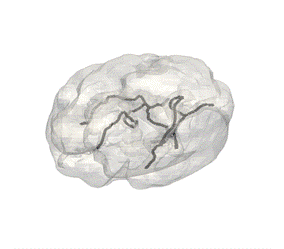
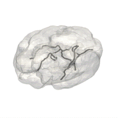
Structural defects in our materials can cause the solar cells we make to degrade too quickly over time, and they can reduce the overall efficiency as well. However, understanding what these defects look like structurally is challenging. One focus in the group has been to use advanced X-ray diffraction techniques, making use of synchrotrons (particle accelerators built to produce high energy X-rays) such as the Diamond Light Source in Oxfordshire, pictured below. In particular, we use coherent diffraction techniques to image strain in our materials with nanoscale resolution. We can then identify specific kinds of defects from their characteristic local strain fields. For example, we have been able to image a network of dislocations (a type of extended structural defect) in halide perovskite crystals. These dislocations are shown in black in the images below.
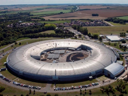
Diamond Light Source in Oxfordshire (photo credits: Diamond Light Source).
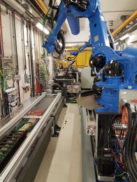
Inside the synchrotron where we do our coherent diffraction experiments.
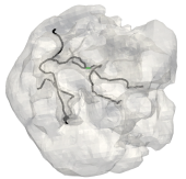
A halide perovskite crystal containing a network of dislocations.
Showcasing I14 capabilities for X-ray fluorescence and diffraction scanning of perovskite materials.
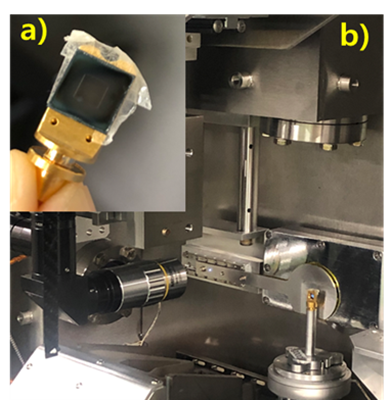
Figure 1 (Inset, a) Perovskite film deposited on SiNx window, b) a mounting prepared sample at I14 sample stage.
The Hard X-ray Nanoprobe beamline (I14) at Diamond Light Source has beam size of approximately 50 nm, making it ideal for investigating the chemical and crystallographic properties of materials at the nanoscale using nano X-ray diffraction (nano-XRD) and nano X-ray fluorescence (nano-XRF) techniques. To conduct measurements, materials are prepared and deposited on silicon nitride membrane (SiNx) windows and mounted on the sample stage compatible with the instrument (Figure 1a). The members of the subgroup have used these techniques to understand nanoscale heterogeneities in these materials. The nano-XRD measurements at I14 revealed that the extent of octahedral tilting depends significantly on perovskite composition, affecting the photo-stability of devices. Additionally, their optoelectronic properties were found to be strongly influenced by local compositional heterogeneity, rather than local strain variations.
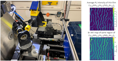
Exploring XANES mapping on perovskite films.
X-ray Absorption Near Edge Spectroscopy (XANES) is an element-selective synchrotron technique which allows you to probe the coordination and local chemical environment around the absorbing atom in a material. At the Microfocus Beamline (I18) at Diamond Light Source, these measurements can be done simultaneously with X-ray fluorescence (XRF) and X-ray diffraction (XRD), while scanning across the surface of the material. This provides spatial information of the material’s chemical composition, environment, and structure. These techniques have been used to study lead halide perovskites to understand how the local chemical and structural environment contributes to the optoelectronic properties and performance of these materials.
Electron-based characterization
Correlative electron microscopy and high-resolution images of various nanoscale structural phenomena
By using a combination of electron and optical microscopy we aim to understand how nanoscale structural inhomogeneities in hybrid perovskite films are related to their performance. By accelerating electrons to high voltages (200 kV) we can produce images of very high resolution, in particular scanning electron diffraction (SED) allows us to gain structural information at low electron doses with a probe size of ~5 nm. From spatially correlating this information with optical techniques, such as photoluminescence microscopy, we are able to learn which structures cause performance losses and seed degradation. Using an electron microscope we can also take atomic resolution images where we learn about both terminations at grain boundaries and crystallographic defects such as vacancies and interstitials.
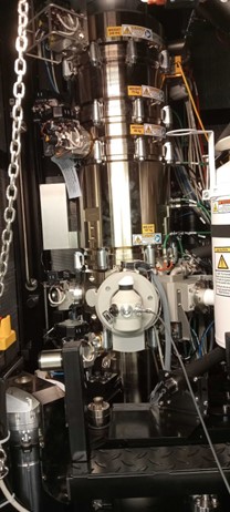
Image of a TEM column
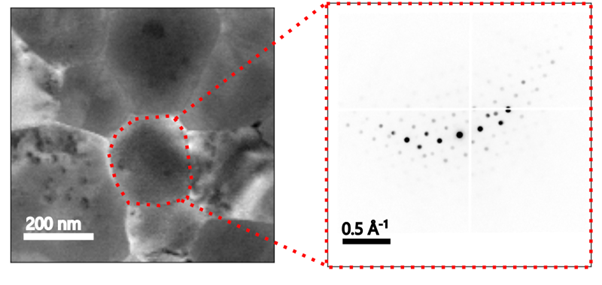
Example of SED data where a diffraction pattern is collected at each ‘pixel’. Region in red shows a particular grain oriented near zone axis.
Related Publications
- K. W. P. Orr et al., Imaging Light-Induced Migration of Dislocations in Halide Perovskites with 3d Nanoscale Strain Mapping, Advanced Materials, 2023, 2305549
- J. Ferrer Orri et al., Unveiling the Interaction Mechanisms of Electron and X-ray Radiation with Halide Perovskite Semiconductors using Scanning Nanoprobe Diffraction,Advanced Materials, 2022, 34, 2200383
- S. Macpherson et al., Local nanoscale phase impurities are degradation sites in halide perovskites, Nature, 2022, 607, 7918
- K. Frohna et al., Nanoscale chemical heterogeneity dominates the optoelectronic response of alloyed perovskite solar cells,Nat. Nanotechnol., 2022, 17
- T. A. S. Doherty et al., Stabilized tilted-octahedra halide perovskites inhibit local formation of performance-limiting phases, Science, 2021, 374, 6575, 1598–1605