
Spectroscopy
We study photophysical processes in novel semiconductors and in optoelectronic devices both to better understand fundamental working mechanisms, and to improve the performance of materials and LEDs or solar cells. The StranksLab has a broad variety of optical techniques across our lab and shared Optoelectronics Group infrastructure - many of them detailed below. One of our key skills is to perform a lot of these spectroscopic techniques with high spatial resolution through the use of optical microscopes. In such a way, we are able to characterise photophysical processes at the local scale, which we correlate with insights from other techniques, such as electron, x-ray, or scanning probe microscopy.
Relevant Publications
- Wei, Z. et al. Photoluminescence microscopy of optoelectronic materials. Nature Reviews Methods Primers 2025, 5(1), 37.
- Stranks, S. D. Multimodal microscopy characterization of halide perovskite semiconductors: Revealing a new world (dis)order. Matter 2021, 4(12), 3852-3866.
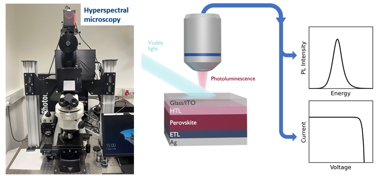
Hyperspectral PL microscopy & in-situ device characterisation
We employ a calibrated hyperspectral microscope to extract emission and absorption spectra with diffraction limited spatial resolution. This enables the extraction of important metrics of material quality, disorder and device metrics. We have customised the setup with operando capabilities, meaning solar cells and LEDs can be operated and their performance directly imaged to offer a complete understanding of device operation and degradation at the nanoscale.
Relevant Publications
- Frohna, K. and Chosy, C. et al. The impact of interfacial quality and nanoscale performance disorder on the stability of alloyed perovskite solar cells. Nature Energy 2025, 10(1), 66-76.
- Fitzimmons, M. et al. Optimised graphene-oxide-based interconnecting layer in all-perovskite tandem solar cells. ACS Energy Letters 2025, 10(2), 713-725.
- Ji, K. et al. Self-supervised deep learning for tracking degradation of perovskite light-emitting diodes with multispectral imaging. Nature Machine Intelligence 2023, 5(11), 1225-1235.
- Frohna, K. et al. Nanoscale chemical heterogeneity dominates the optoelectronic response of alloyed perovskite solar cells. Nature Nanotechnology 2022, 17(2), 190–196.
- Kahmann, S. et al. Taking a closer look – how the microstructure of Dion–Jacobson perovskites governs their photophysics. Journal of Materials Chemistry C 2022, 10(46), 17539–17549.
Time-resolved confocal PL microscopy
With a confocal PL microscope, we can map photoluminescence (PL) intensities and lifetimes with sub-micrometre spatial and sub-nanosecond time resolution. By scanning both the excitation and the emission over a sample area, a time-resolved PL map can be readily obtained. By fixing the excitation position while scanning the emission, we can perform diffusion mapping. The resulting diffusion map reveals valuable information on local exciton transport in the materials, such as the diffusion coefficient both laterally and vertically. Furthermore, our setup is equipped with a pulsed fs-laser with tunable wavelengths ranging from 340 to 1300 nm. This allows us to acquire PL maps with two-photon (2P) excitation, offering spatial resolution in the z-direction down to 1 μm. As conventional one-photon PL mapping is often limited to the sample surface due to a shallow penetration depth, 2P PL mapping is a powerful technique to visualise local properties deep within the bulk of a material
Related Publications
- Cho, C. et al. Efficient vertical charge transport in polycrystalline halide perovskites revealed by four-dimensional tracking of charge carriers. Nature Materials 2022, 21(12), 1388–1395.
- Baldwin, A. et al. Local Energy Landscape Drives Long-Range Exciton Diffusion in Two-Dimensional Halide Perovskite Semiconductors. The Journal of Physical Chemistry Letters 2021, 12(16), 4003-4011.
- Stavrakas, C. et al. Visualizing Buried Local Carrier Diffusion in Halide Perovskite Crystals via Two-Photon Microscopy. ACS Energy Letters 2020, 5(1), 117-123.
- Stavrakas, C. et al. Probing Buried Recombination Pathways in Perovskite Structures using 3D Photoluminescence Tomography. Energy & Environmental Science 2018, 11(10), 2846-2852.
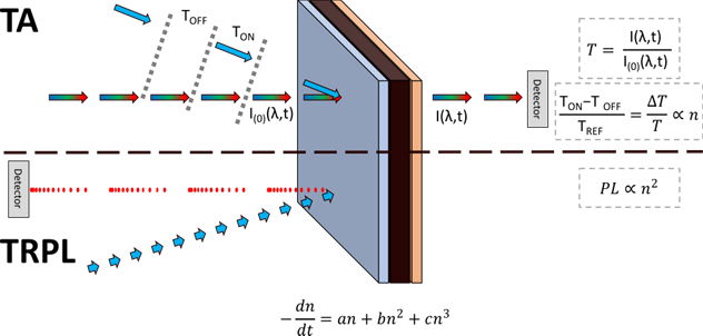
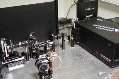
Carrier dynamics in devices/layered structures through time-resolved techniques
As a research team studying semiconductors and device stacks, we utilise ultrafast transient absorption (TA) and time-resolved photoluminescence (TRPL) techniques to elucidate charge carrier dynamics and probe interfacial recombination, on a time scale ranging from femtoseconds to microseconds, in our OE FastLab based in the Maxwell Centre. TA observes changes in the excited state carrier population through changes in the probe pulse (380-1800 nm, UV to IR) transmission as a function of time after photoexcitation with up to 100 femtosecond resolution, while TRPL measures the time evolution of sample luminescence after excitation. These techniques grant a better understanding of the mechanisms of carrier transport and recombination within semiconductors. These findings can then inform design and performance optimization for devices by elucidating mechanisms of efficiency improvement or degradation pathways.
Related Publications
- Boeije, Y. et al. Molecular Engineering of Interlayer Exciton Delocalization in 2D Perovskites. Journal of the American Chemical Society 2025, 147(35), 31541–31557.
- Boeije, Y., Van Gompel W. T. and Zhang, Y. et al. Tailoring Interlayer Charge Transfer Dynamics in 2D Perovskites with Electroactive Spacer Molecules. Journal of the American Chemical Society 2023, 145(39), 21330–21343.
- Feldmann, S. et al. Photodoping through local charge carrier accumulation in alloyed hybrid perovskites for highly efficient luminescence. Nature Photonics 2020, 14(2), 123–128.
- Bowman, A. R. et al. Microsecond Carrier Lifetimes, Controlled p-Doping, and Enhanced Air Stability in Low-Bandgap Metal Halide Perovskites. ACS Energy Letters 2019, 4(9), 2301–2307.
PLQY and Operando PL spectroscopy
The Operando PL system measures the absolute PL spectra while doing the J-V scanning of a perovskite solar cell under 1-sun equivalent illumination. This allows for a comparison between the internal (QFLS-V) and external (J-V) device performance of solar cells under operating conditions. Analysis based on this measurement quantifies the charge recombination loss and extraction efficiency in direct correlation to device parameters (VOC, JSC, FF) This setup can also be used for electroluminescence measurements and general film QY measurements.
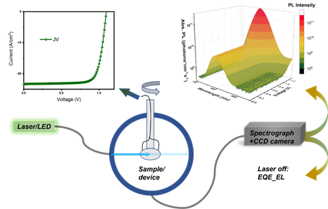
Schematic drawing of the operando PL setup
Related Publications
- Xu, W. et al. Unveiling the Role of Guanidinium for Enhanced Charge Extraction in Inverted Perovskite Solar Cells. ACS Energy Letters 2025, 10(6), 2660–2669.
- Li, S., Xiao Y., Su R., and Xu, W. et al. Coherent growth of high-Miller-index facets enhances perovskite solar cells. Nature 2024, 635(8040), 874–881.
- Bowman, A. R. et al. Extracting decay-rate ratios from photoluminescence quantum efficiency measurements in optoelectronic semiconductors. Physical Review Applied 2022, 17(4), 044026.
- Feldmann, S. et al. Photodoping through local charge carrier accumulation in alloyed hybrid perovskites for highly efficient luminescence. Nature Photonics 2020, 14(2), 123–128.
Photothermal deflection spectroscopy
Photothermal deflection spectroscopy (PDS) is an experimental method enabling sensitive optical absorption measurements. It is based on periodic photoexcitation of the material causing alternating temperature gradient at the surface, further probed by deviation in the optical path of a laser beam passed close to the sample (thermal lensing/mirage effect). Due to working principles fundamentally different from the classic approach for measuring optical absorption, PDS surpasses UV-VIS spectroscopy in terms of sensitivity, dynamic range, and being insensitive to light scattering. We use PDS for investigating sharpness of the absorption edge, representing electronic and structural disorder and quantized by the Urbach energy. Apart from being a relevant parameter from a pure materials research perspective, it is known to be correlated with the open-circuit voltage deficit in solar cells. The extraordinary sensitivity of PDS is also useful for identifying defect-related absorption and other weak features in the sub-band-gap energy region.
Our PDS system shared in the OE group covers a broad spectral range between 0.6 and 4.0 eV, can measure thin films as well as single crystals, and due to its modular structure remains fully customizable to allow extended experimental configurations (e.g. simultaneous photoluminescence detection, electrical or side light biasing, solution-based measurements).
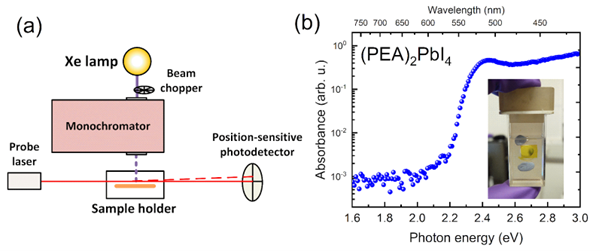
- PDS setup schematic, (b) exemplary spectrum of evaporated (PEA)2PbI4 two-dimensional perovskite layer. The inset shows the sample holder filled with a heat transfer liquid.
Related Publications
- Boeije, Y., Van Gompel W. T. and Zhang, Y. et al. Tailoring Interlayer Charge Transfer Dynamics in 2D Perovskites with Electroactive Spacer Molecules. Journal of the American Chemical Society 2023, 145(39), 21330–21343.
- Liu, Y. et al. The Electronic Disorder Landscape of Mixed Halide Perovskites ACS Energy Letters 2022, 8(1), 250–258.
- Andaji-Garmaroudi, Z. et al. A highly emissive surface layer in mixed-halide multication perovskites. Advanced Materials 2019, 31(42), 1902374.
Modelling carrier dynamics
Analysis of decay curves in time-resolved PL and other transient techniques quickly becomes convoluted in perovskite films and devices. After photoexcitation, there are multiple processes occurring simultaneously (Auger, bimolecular and SRH recombination, diffusion, trapping and detrapping of carriers, etc.). Resolving the contributions of these processes is non-trivial and great care has to be taken when thinking about how we fit these decay curves. In our group, we develop models and fitting procedures to extract carrier recombination constants. We have recently been developing Monte Carlo analyses - a technique that samples vast parameter spaces to find the best fit parameters. This is advantageous over classic fitting techniques which are prone to fall into local minima, whereas Monte Carlo walkers can ‘step’ out of local minima to find the true global minimum of the parameter space. In our testing of this method we have simulated decay curves according to varying physical models, which highlights the greater or lesser impact of parameters on the overall fit.
Related Publications
- Bowman, A. R., and Stranks, S. D. How to characterize emerging luminescent semiconductors with unknown photophysical properties. PRX Energy 2023, 2(2), 022001.
- Bowman, A. R. et al. Extracting decay-rate ratios from photoluminescence quantum efficiency measurements in optoelectronic semiconductors. Physical Review Applied 2022, 17(4), 044026.
- Nagane, S. et al. Tetrafluoroborate-Induced Reduction in Defect Density in Hybrid Perovskites through Halide Management. Advanced Materials 2021, 33(32), 2102462.
Cryogenic measurements
We are interested in the fundamental photophysical properties of our novel semiconductors. In a variety of cases, we thus extend our powerful spectroscopic experiments with the capability to vary the sample’s temperature. Typically, such experiments are conducted over a range from room temperature down to 4 Kelvin, for which we employ liquid helium cooled cryostats. A special microscope cryostat allows us to also perform the high resolution imaging experiments under such conditions.
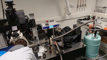
Our hyperspectral microscope in operation with the liquid helium cryostat. The Coolant is contained in a large dewar on the right, which is pumped into the cryostat via a long transfer line.
Related Publications
- Dubajic, M. et al. Dynamic nanodomains dictate macroscopic properties in lead halide perovskites. Nature Nanotechnology 2025, 20(6), 755-763.
- Guo, D. and Selby, T. A. et al. Visualizing Nanodomain Superlattices in Halide Perovskites Giving Picosecond Quantum Transients. arXiv preprint 2025 arXiv:2502.13609.
- Kahmann, S. et al. Taking a closer look – how the microstructure of Dion–Jacobson perovskites governs their photophysics. Journal of Materials Chemistry C 2022, 10(46), 17539–17549.
- Stavrakas, C. et al. Influence of grain size on phase transitions in halide perovskite films. Advanced Energy Materials 2019, 9(35), 1901883.
Circularly polarised spectroscopy
Chiral structures and chiral semiconductors can offer circularly polarised transitions. Luminescence, for example, can predominantly occur with right-hand symmetry or with left-hand symmetry. Whereas general spectroscopic experiments only measure signal intensity, we equipped several of our experiments with the capability to identify and to study circularly polarised light. In the simplest case, a combination of quarter-wave plate and linear polariser is used to render a multi-purpose spectroscopic set-up sensitive to polarised light. Such measurements are complemented with circular dichroism.
Back focal plane imaging
In addition to our extensive real-space microscopy capabilities, we employ back focal plane (BFP) imaging. In this technique, the objective lens is focused on a sample, and the back focal plane of the objective is imagined by inserting an additional (Betrand) lens in the infinity space between the objective and the tube lens. The resulting image of the BFP contains information about the sample's spatial frequencies and about directionality of emission/reflection. By switching the imaging detector to a spectrometer, we are furthermore able to simultaneously measure the angular and wavelength dependence of reflected or emitted light.